Hello all,
I realize it has been a couple of months since I posted anything here.
Just finished the heaviest course my study has to offer successfully, this is mostly the reason why I wasn’t able to do anything for this project.
I would like you to know that even when I’m not posting anything here, I haven’t forgotten the project.
It’s just the fact that I have a busy life and it’s hard to combine all the stuff I am working on.
Anyways, I have something to share.
I managed to write the library for the storage chip, and I was finally able to succesfully solder the e-paper to my custom made dev-board:
You can see in the video that the display got damaged from the numerous soldering attempts (especially those when I did not have the devboard yet).
This setup will do for now while testing basic functionalities like reading from storage and uploading to the display.
I also have a devboard for a chip that is available as a really tiny wafer level package, so if I can control it with this devboard I coulld use this 2x2mm chip in the final implant.
Now I finally have a working system again, it might be time to test with some skin analogs.
Chicken skin was recommended several times in this thread, but if any other suggestions arrise please share them!
Again, please excuse me for not posting for so long.
I SHOULD have more free time now to keep working on it.
Decided to post a small progression post here to show you the progress I made last 2 weeks.
I am not sure if I should keep posting new replies or edit the older one, please let me know which one you prefer.
I would like to keep you updated as much as possible since I did not very regularly do that in the past, but I also do not want to spam you.
The driver for the storage module was already written by me some time ago, I removed some bugs and improved query efficiency.
Now the e-paper can update from the external storage, not relying on the MCU’s internal storage.
Here is a video of the display cycling through 10 pre-loaded images onto the storage IC:
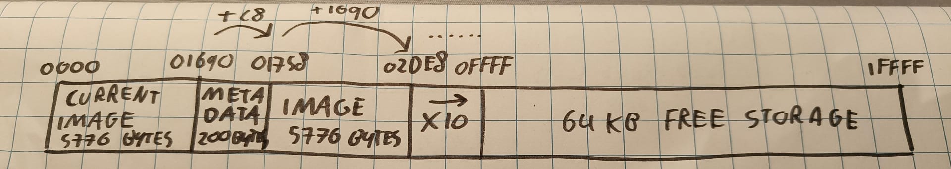
I also made a concept memory map of this IC to make the integration with the NTAG I2C easier later on:
You can see that the memory is seperated into 2 seperate compartments.
The first 64KByte is used for the storage of images and metadata.
The first block is the current selected image, this is saved here so that the user could also just refresh the display from memory if the image faded over time.
Next to that you can see 200 bytes of metadata and 5776 bytes for the image times 10.
You can store 10 grayscale images into this memory sector.
The free 64KBytes could be used to store important/personal data.
All of this memory can be written to with the pass-through mode of the NTAG I2C.
If you have any ideas/suggestions/questions, please let me know.
Cheers!
P.s. These were some random images I had on my desktop, yeah some of them are weird
Glad you’re still working on it. Just to loop back, I know you were planning to use the NTAG I2C+. Have you determined how much current and at what voltage range you need for the display? After further testing I determined that the output voltage of the NTI2C+ droops considerably under load.
When I tested with an ATTiny84 some time ago, I believe I measured something like 6mA at 3.3V, running at 1MHz (during refresh, less than 0.1mA when idle).
I was hoping we could pull at least 10mA from a NFC enabled smartphone, since in theory it should be able to provide up to 15mA over NFC.
Guess ‘in theory’ is always too good to be true…
I recall you saying something like it not being compatible with iOS, but I’m not sure any more if that was you or if I heard it somewhere else.
No not at all, I much rather prefer SPI for its stability and speed.
I thought the NTAG I2C is all there was, but if you know of a chip that can do it over SPI I would much rather do that.
I don’t know why, but for some reason I find SPI easier to work with as well, guess it’s just because of more experience.
The storage IC and display already run of SPI and they don’t intervere with each other, so if we could also add the NFC receiver to that it would be amazing!
Yeah, that’s a lot for NFC energy harvesting. We could maybe do that with the NTAG 5, or 2-4 NTI2C+. If not then one fallback option is my Qi receiver design that can source 750mA at 5V from a phone with battery share.
I’m not sure if that’s still true. the NTAG 5 uses ISO 15693, not the usual ISO 14443a. iirc there have been recent compatibility updates though. Lemme go check with the team.
Well if we’re using the NTI2C+ or NTAG 5, you’re stuck with I2C somewhere in the mix, because that’s all they support. We could send NFC commands from the phone, have them translated into I2C, then have a microcontroller in the implant translate them to SPI if that’s necessary.
This was my plan to begin with, in order to upload to the storage IC the I2C passthrough data needs to be fed to the MCU which will then put it into storage.
I don’t think I actually told already which storage IC I am using, it’s a 128kByte (1M for the bit-oriented people) FRAM storage IC on wafer level.
It’s blazing fast, I was able to write 64KByte from an ESP32’s memory to this IC in less than 20ms.
The ESP32 runs on 240MHz of course, which is not archievable at the power levels we are working with, but it’s still nice.
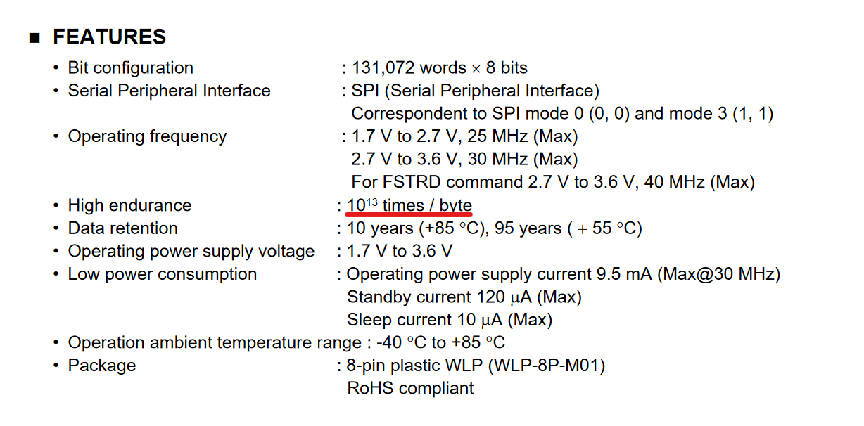
Why FRAM? Unlimited endurance and resistant against nuclear radiation (think of X-rays and such)
Against reads, but very susceptible to write fatigue. I get where you’re coming from, and that’s a good call. Just be wary of the maximum write stability. You’re going to need to implement some wear leveling
10^13 write operations (read: unlimited).
I think you are confusing EEPROM and FRAM.
FRAM is a relatively rare storage technology which is as fast as RAM, but also non-volatile. It stores data in crystals.
It has been half a year, and I am sorry for that.
I have been very busy with my studies and job, but since the summer holidays are coming up, I finally have some free time to work on my private projects again!
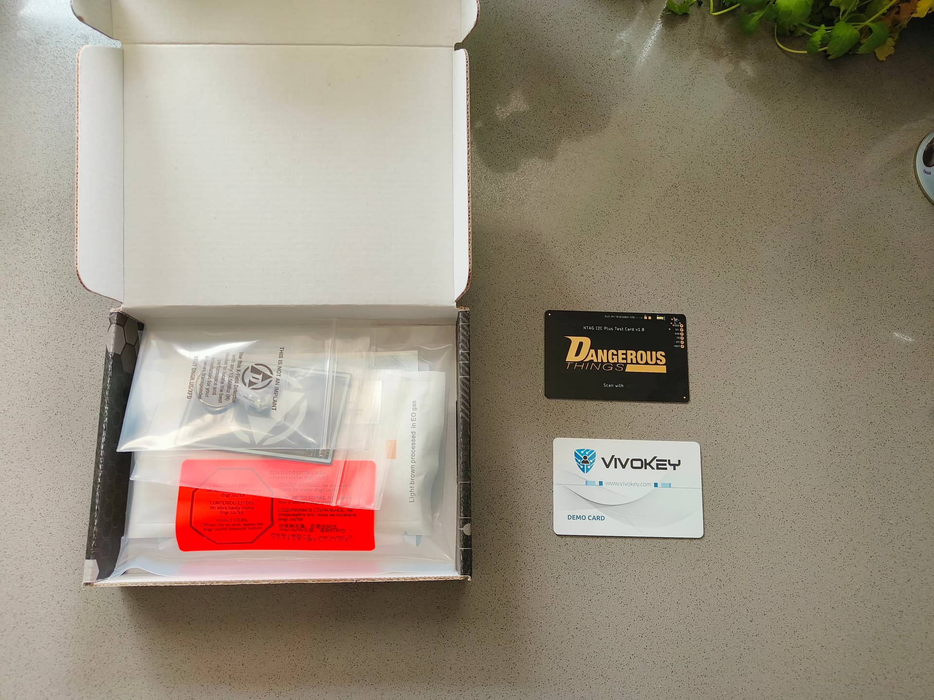
That is why I have finally made the decision to place an order at the shop for a xSIID green implant, an I2C test card, and a VivoKey devkit.
The first and third product are just for myself, but the I2C test card is going to become useful for testing out my E-Paper concept.
I have really developed myself in terms of PCB design and overall engineering skills, so I am full with new energy to get working on this project again!
I can offer no guarantees on the (speed of the) development process since I am a busy guy, but I will try to give it my best shot during the free time that I have!
I just wanted you to know that I am back at it.
The VivoKey Dev kit is two cards with the same chip in them as the VivoKey Spark. I think they use the chip from the first version of the Spark, but it might be the v2 chip that is in the Spark 2.
The Spark can’t really be programmed with data. Cool implant and some fun things are being developed around them (identity and authentication), but I don’t think they would be relevant for your project.
No worries mate, it happens. I’ve been at this for years. Not coming back at all is always going to be more disappointing than any delay forced by life. Persistence is key.
That’s exciting to hear! Feel free to reach out if you want to collaborate on any PCB design stuff, or just need some money to get things off the ground.
I am aware of this, I just thought that the idea of a personal identification chip is really cool and futuristic. Since I am not sure what it does yet, I decided to get the test kit instead of an implant first. For the xSIID, I know these types of chips and their versatility, I got no problems with those being inside my body.
That is really nice of you, I still have your discord so I know how to reach you. I might have a possible replacement microcontroller which is tiny and easier to develop for. I still need to confirm it’s power characteristics, I am not sure if it can beat the NXP KL03 series as discussed earlier.
I will now look for someone in the Netherlands to place my xSIID in my hand.
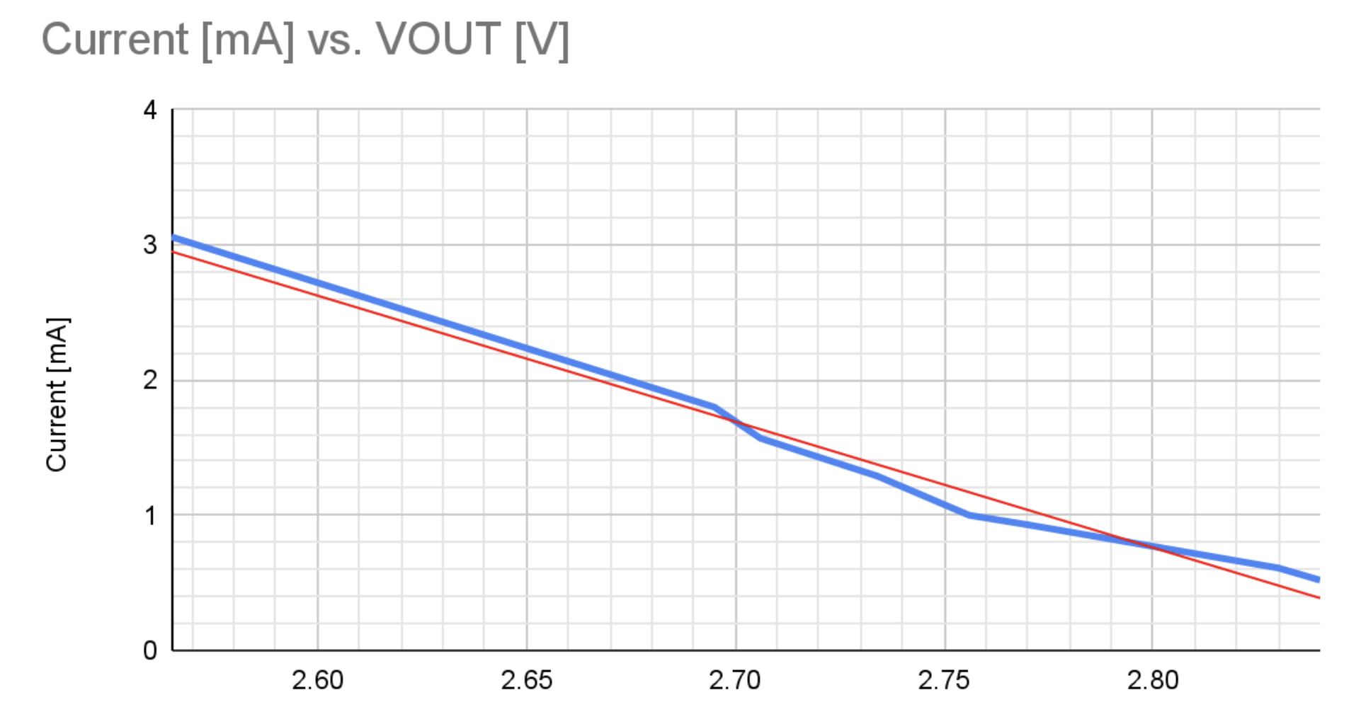
Regarding the I2C devcard, I briefly tried it and it works with my phone! To conserve all the energy, I will disable the LED and see if I can power any of my MCUs from it.
Edit: I was able to measure up to 2.65V on the test card. This should be enough to power a simple low-power microcontroller (although this voltage might drop when pulling too much current). The display requires 3.3V, so I would have to find a solution for that. I do not want to implement a boost converter since it will likely take up too much space and it can cause overheating issues (which are REALLY undesirable inside of your body).
Unrelated to this topic: I am a bit confused by the VivoKey devkit cards. If I understand it correctly, they should be able to have some cryptographic capabilities. When scanning them with a NFC scanner app, they only redirect to a vivokey web page that can hold my contact info when set up in the app. All the app seems to do is upload my data to an external server where the card redirects to, without modifying the tag itself. What am I missing here?