I had another look at the ATtiny sleep mode and they seem to have a power-down mode (can be woken with an interrupt or reset) that only uses 0.1uA which is within budget I think (check this mess I guess)
I also ordered a piezo to test if we could do alarms or timers using the RTC to provide interrupts, just a concept really (if that doesn’t work maybe we could have exposed contacts and zap you?). I was also thinking of more than 1 magnet sensor so we can have multiple functions (date, time, timer, something fun).
What does everyone think of having a second microcontroller (like a bootloader) so we can reprogram the main MC over NFC?
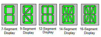
A 16 segment display wouldn’t use any more power than a 7 in normal operation so I think we should go with that
A 16 segment will require either a hardware driver (more chips, higher power consumption) or a lot more I/O lines. (Possibly more than are available on an ATTiny85)
Obviously it is capable of displaying more complex sigils, but if the idea is just for an implantable clock then it really isn’t necessary.
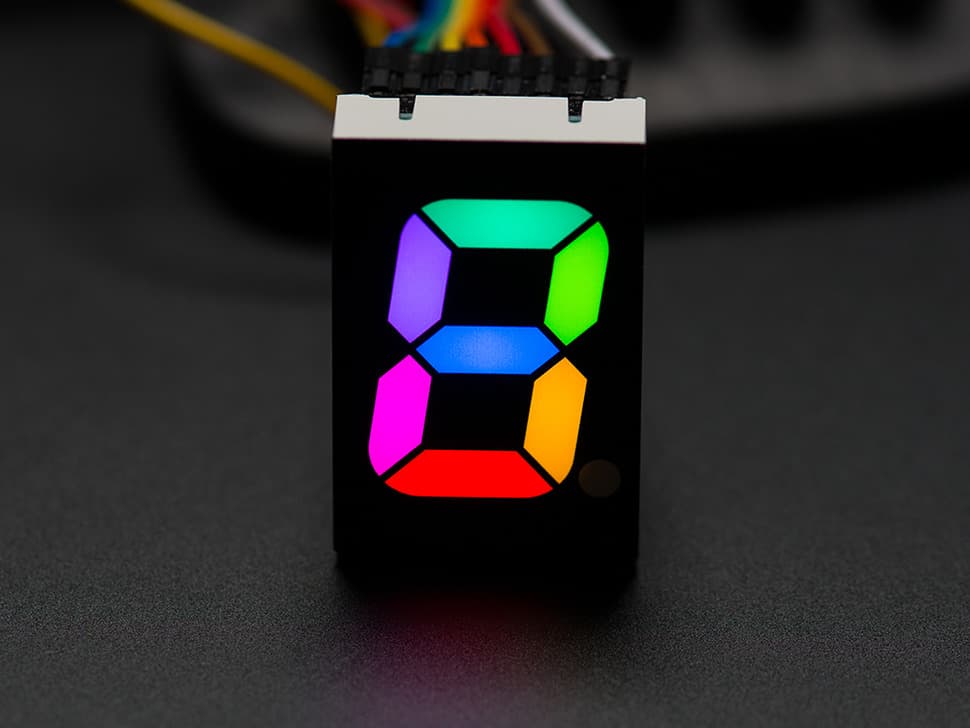
Edited to add: personally I was looking for relatively large but low profile LEDs as that would make implantation easier
I’m looking at the 88 as a potential candidate even without the 16seg and it would have enough, and I took apart a 7seg yesterday and it has 2 LEDs per segment, I assume in a 16seg there would be 2 for the large and 1 for the small segments so no more power required
I was thinking of having another ATtiny (smallest one available) that is activated with the NFC chip and acts as a bridge and programmer for the main chip, does anyone know if we could have a single chip program itself? It’s probably possible but self modifying code seems easy to brick
Another thing is would we need a DC-DC step up? and does anyone have a low power suggestion?
Looks like there are STM32 variants that have built in RTCs. Some of the sleep modes support running the RTC simultaneously. Then you just wake the device t with an interrupt from sensors, (like a hall effect or vibration sensor).
Page 84, Standby mode with RTC on uses about 2.7uA which we can manage, and if we can put it into vbat mode we could get down to 0.73uA but this would require another chip that probably uses 2uA or more. This looks good I’ll get one for testing, any preference for which?
Does anyone have Android and/or IOS experience? We need an app to sync the time, configure things (maybe even dynamic configuration, ie the implant sends a template for what can be adjusted), and upload firmware over NFC
I’m happy to try my luck if not
NTAG 5 can output more current for the energy harvesting, it has much better range because it’s ISO 15693 instead of the standard ISO 14443a, it’s I2C communication has many more options, and it’s a much more capable chip that can support cryptography if we want to add it.
I was hoping we could find a workaround instead of using an app. Apps have to stay compliant to the Play store to stay public, and they have to stay up to date for newer versions of Android. What would have a longer lifespan would be a series of raw commands we can send from any device, independent of an app, and a program that can run on the computer using any PC/SC compliant USB reader (like an ACR-122U) to handle if you ever need to do in-application programming. That will be more future proof, so anyone with the correct documentation can make it work, without us needing to build and maintain an app.
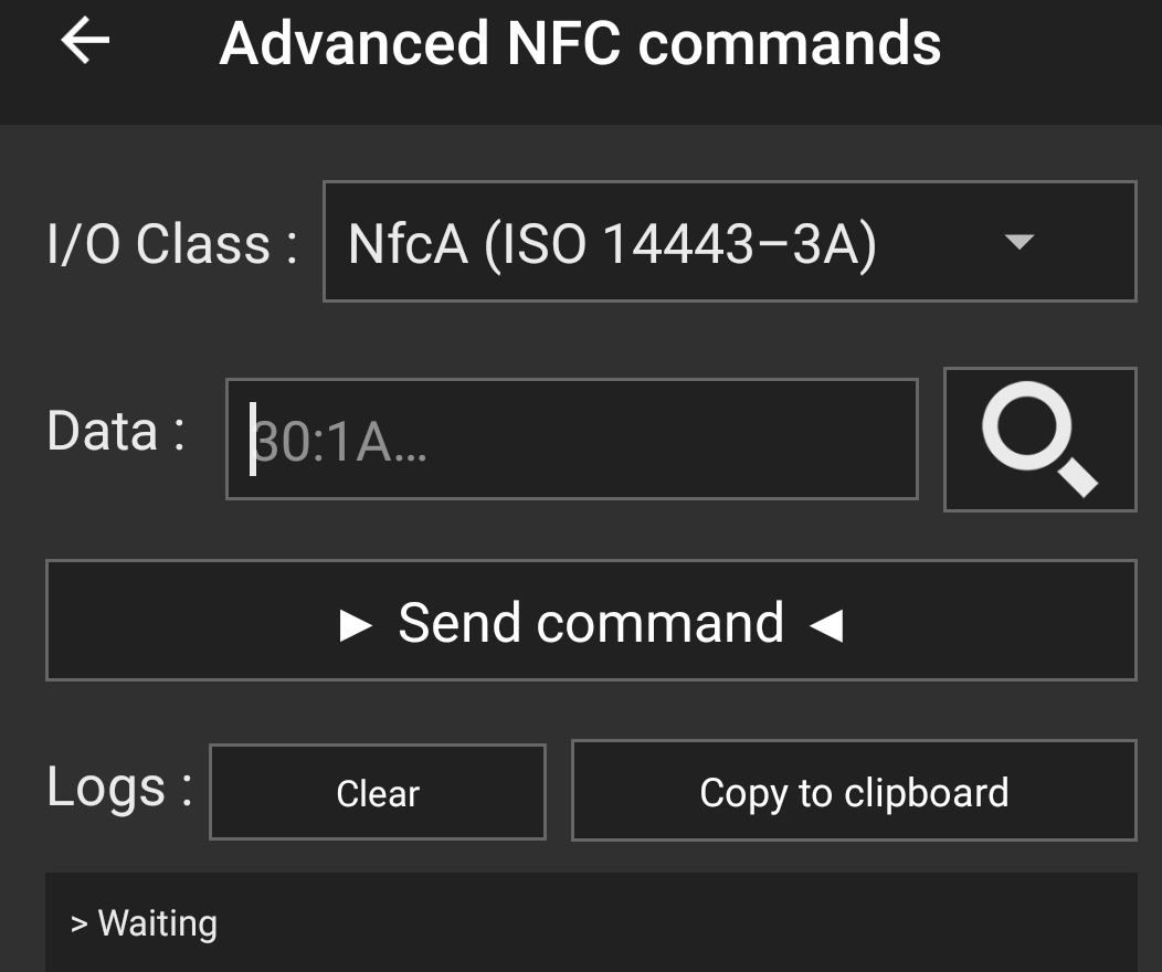
But what I mean is how will we send them? Raw NFC, or NDEF records? Now that I think about it if the writer check that it wrote properly that might make things difficult