TL;DR - The first batch of xSIID made December 2019 were formatted to try to use all 2k of memory across two 1k memory sectors for NFC applications, but the NFC stacks built into Android and iOS phones don’t know how to properly read multiple memory sectors in NFC Type 2 chips. Future batches are formatted to only use the first memory sector which is 1k for NFC applications. The remaining 1k is still readable and writable by phones, but only with a custom smartphone app that can directly address this memory.
And nooowwwww…

Ok.. so here goes.. NXP made the NTAG I2C chip used by the Dsruptive SiiD module which we purchased from them to make the xSIID implant. That chip comes in 1kB and 2kB flavors. Dsruptive chose to get the 2kB because why not? Well this is why not…
The Ultralight (and later NTAG) style of tags with 4 bytes per memory page arranged as contiguous memory had the UID data and some important locking information and other info all in the first few pages of memory.. then at page 03 the writable memory started with page 03 being OTP (one time programmable) bytes and pages 04 to the end page (how many pages existed depended on total memory size) were openly writable you’d use all this memory for your application.. usually by writing some kind of special application ID to the OTP bytes in page 03 and then locking that special page.. this way your application could read just page 03 and know immediately if the tag was worth reading or not (is this a valid tag for my application?).
With the advent of NFC and the Type 2 specification, Ultralight style tags with a specific memory configuration were deemed “type 2 compliant” if properly “formatted” for use with NFC. What does that mean? Well, it means when you want to format the tag for use as an NFC tag, you would write a well defined “NFC capability container” to memory page 03 with 4 special bytes that defined that the tag memory was to be used for NFC, the NFC spec version, and the amount of memory to be used for NFC.
Capability container
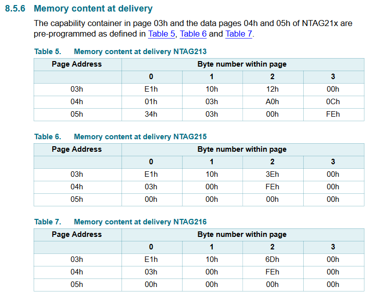
The capability container is where things go a little sideways. Let’s have a look at the NTAG21x specification sheet for a better understanding of the CC (capability container).
As you can see, byte 02 defines the “memory size” available for NDEF messages, not necessarily the size of the chip’s user memory. I won’t go into the maddening nonsense tucked away inside NXP’s documentation on how to calculate the capability container’s byte 2 value because it’s contradictory between documents and none of them share the same result when calculated, so I won’t perpetuate their misinformation here. What is well known is that the common memory size for a “1kB” (but really 888 bytes) NFC Type 2 chip with 4 byte memory pages is that byte 2 should be 0x6D. This is the value that NXP suggests, writes by default to their NFC formatted chips, and it is the value that Android and iOS operate well with (more on that later).
Split memory sectors
The concept of memory sectors was utilized in old legacy Mifare S50 1k and S70 4k “classic” chips. Memory in these chips is organized into blocks, there are several blocks per sector, and there are several separate sectors that comprise the whole of the chip’s memory capacity. Each sector could be secured with it’s own set of keys and access permissions. In this way, in theory, multiple applications could claim a sector or sectors for itself, but leave other sectors alone which other applications could use for their own purposes. Even so, this never worked because it still required too much coordination between app developers, so every chip ended up being pretty much used as a single purpose device. Possibly because of this, by contrast, the Ultralight and NTAG21x chips don’t bother with that and have a contiguous memory structure arranged as a series of 4 byte pages, all in a single “sector”.
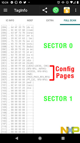
The NTAG I2C 2k chip is different however. The first “1kB” of memory is constructed just like an NTAG216 chip’s memory, with basic data in the first 3 pages (page 00 to page 02), then a capability container stored in the OTP (one time programmable) bytes of page 03, then pages 04 - E1 are user writable memory, able to be used for NFC data (called NDEF data). But NTAG chips have more data after page E1, and these pages E2 - E5 contain “configuration data” or as I call them “configuration bytes”. This is where the NTAG21x password feature lives, amongst other important things. This is one reason why the “memory size” value of byte 02 in the NFC Capability Container is so important. The NFC application writing data to your chip must not accidentally overwrite this section of memory, thinking it is freely available user memory.. otherwise bad things can happen if you write random data over critical configuration data.
Since the NTAG I2C chip used to make the xSIID implant has 2kB of memory, and the first 1kB of memory exactly mimics that of the NTAG216 chip, how do we get 2kB of memory? Well, they put the additional 1kB into a new sector.. sector 1.
Hrm..
Memory problems
When reading the documentation and NFC Type 2 specification document (which is a spec doc you must pay for, so we can’t link to it here), we see this as the only reference for calculating a capability container for a Type 2 chip.
So, you can see the calculation is simple.. 8 x byte = size .. and if we look at the NTAG216 with it’s 888 bytes of user memory, we see the accepted value of byte 02 being 6D, which is 109 in decimal, which means 8 * 109 = 872.. 872? .. huh? Why not 110 to get 880 bytes, or 111 to get all 888 bytes?
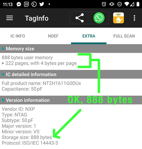
The documentation for the NTAG216 as well as NXP’s own TagInfo app shows the NTAG216 has 888 bytes of “user memory”, but nowhere does it define exactly what that means.
The whole of the NTAG216’s memory has pages 00 - E6 which means if we adjust for base 0, there are E7 memory pages with 4 bytes each, or 231 pages times 4 bytes = 924 bytes total.. but the NXP app indicates there are 222 pages of “user memory”.. so let’s try to figure this out.. and no, the little arrow thing next to the page count indicator is not a drop-down, it’s just some engineer’s whim to use a commonly known symbol for “tap here for more info” as a useless indicator. Gee. Thanks.
So if we remove the first 3 pages (00-02) we’re down to 228 pages.. now let’s remove the config bytes at the end.. those are stored in pages E2 - E6 so that’s another 5 pages down. to 223.. so that leaves the Capability Container in page 03.. even though it is writable by the user by default (we disable that though at the factory), they don’t count it as “user memory”.. so now we have our 222 pages.. but that’s still 888 bytes.. so why not set up your CC with a byte 2 value of 6F to indicate you can use all 888 bytes for NFC data?
When I pressed NXP about this, they said, and I quote:
“6D was the commonly accepted value for 1kB sized tags, and if you want your chips to work with the most number of NFC devices, you will use 6D in your Capability Container and forgo the use of the last few pages of memory space.”

Sooooo.. we have a clear standard that easily defines a very simple approach to calculating memory size to earmark as NDEF data storage for NFC applications.. and.. the industry.. i.g.n.o.r.e.s. it?? .. gotcha.. ok.. uhhh. okk.. so.. well ok.
My mistake
When it came time to code up a programmer for our factory line to use on the xSIID before putting the chips into syringes and sterilizing, I made an assumption. I knew I could not necessarily trust the NFC standard for calculating byte 02 for memory size, so I fished for an answer from support reps and people in the industry, and I got one. The commonly accepted byte 02 memory size value for 2kB chip was EA, or 234 * 8 = 1872 bytes. The actual memory size was 222 pages or 888 bytes for sector 0, while sector 1 had no special pages and a range of 00 to FF or 256 pages * 4 = 1912 bytes.. so 1872 seemed.. safe.
I set about compiling the programmer code and sent it off to the factory and that’s what the first xSIID batch was programmed with.
The reckoning
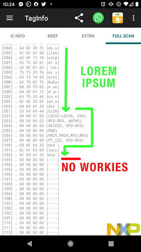
Even before the xSIID chips were done with sterilization, problems began to arise. These problems presented themselves at first like a problem with TagWriter, NFC Tools, and other NFC apps.. specifically their ability to write more than 1kB of data. This presented itself when I was attempting to write 1600 bytes of Lorem Ipsum to a test chip..
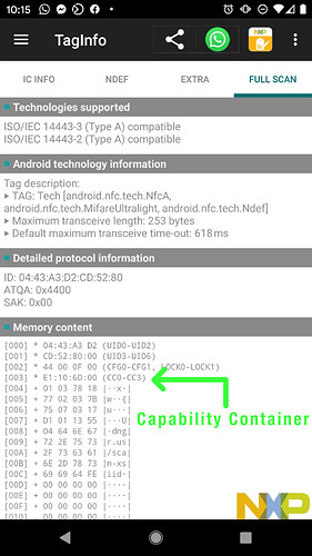
You can see the data writes to the end of the sector 0 user memory (page E1 in this screenshot was overwritten later with SiiD).. and then it jumps to sector 1 and continues to write, but only for 3 pages, then stops. The jump to sector 1 to keep writing data requires a specific set of commands that must be issued to the chip, so the fact any data exists on those pages at all means that TagWriter and the Android OS itself are both capable of accessing sector 1.. but something went wrong and the write stopped at page 102.
Another odd result was that tags written in this way with data that extended beyond sector 0 were no longer readable by Android. Attempts to read this tag with TagInfo or really any app, including the OS level intent processor itself, always resulted in an “NFC Error” dialog pop-up toward the bottom of the screen that would quickly fade away, with all my hopes and dreams going with it.
Luckily these tags could be recovered by directly writing to them with the ACR122U and some quickie software I whipped up, and once the offending, corrupted NDEF message was removed, the tag worked normally again.. until the next time an NDEF message extended beyond the bounds of sector 0’s user memory. I pressed NXP to fix the “write bug” they had in TagWriter, but through weeks and weeks of back and forth, the truth finally came to be realized..
The problem defined
It turns out there was a bug in TagWriter, and the NDEF message was being corrupted. They informed me that they would fix that bug, but it would not solve my problem. After even more back and forth, it came to light that the reason that Android (and iPhone at this point) were saying “NFC Error” and unable to read or really access the tag at all had to do with the fact that neither OS had NFC stacks capable of reading multiple sectors from a Type 2 NFC tag.
That meant that the OS was reading the tag and seeing the capability container.. understanding that there was approximately 2k of memory, reading the NDEF message, looking at the payload length stored right at the start of the first NDEF record inside the NDEF message and seeing ok, about 1600 bytes.. cool no prob.. then going page by page to read it… successfully skips over the configuration bytes in pages E2 to E6.. but then tries to access page E7 which is a special page for the NTAG I2C but doesn’t exist in the NTAG216.. then goes “ah great..” and tries for page E8 and gets an error.. so it panics.. tosses up a user error.. and aborts.. not even an NFC app on the phone can do anything with the tag because the RF session with the chip has been dropped completely.
What’s the answer?
The answer from NXP was to limit NFC application memory for NDEF messages to just sector 0.. in short, treat it like an NTAG216 and format the Capability Container with byte 02 being set to 6D… or.. convince Android and iOS to properly recognize the gap and jump over to sector 1 to keep reading the NDEF message to completion.
New batch
New batches of xSIID manufactured after Dec 2019 are programmed in this way. Only 1k of memory is accessible for NFC applications which rely on NDEF data. It is still possible, even on phones, to read and write data to sector 1, however those functions will require special commands to be sent to the chip, and that is only possible if you make your own app.
Fixing old xSIID
You might ask if it’s possible to fix the old xSIID capability container to set it with a new size byte. The answer is no, twice. The first no is due to the fact that page 03 where the capability container lives uses OTP bytes which are one-time-programmable. They come from the factory with all 8bits in each byte set to 0.. but if any bit in page 03 is flipped to 1 then it can never go back to 0.
The “bad” value is EA in hexadecimal, which is 11101010 in binary. The “good” value is 6D, or 01101101 in binary. Reading from left to right, we can see that the first bit of the bad value is 1.. and the first bit of the good value is 0.. already we are stuck.. we cannot go back.
The second no is due to the fact that during manufacturing, we don’t want anyone mucking up page 03 goin around flippin bits that can’t be unflipped.. so we lock protect it read-only using the static lock bit assignment in page 02. This means page 03 is forever set and cannot be changed one way or the other.
The only fix for older xSIID with byte 02 of the capability container set to EA would be for Android and iOS to both fix their NFC stacks to properly read all the data from these types of multi-sector Type 2 NFC tags.
Fixing broken NDEF records
Of the older batch with the miscalculated CC size, it is possible to overrun the first 1k of memory and leave the NDEF message fundamentally broken… or rather broken to the phone which does not properly understand how to bridge the gap between memory sectors to continue reading the NDEF message. This tends to “hard break” the phone’s ability to interact with the tag at all. That’s because even if you are trying to use an app like TagWriter or NFC Tools, when you scan a tag the phone’s OS is going to do some poking around first before handing over any control to the app.. and that process of poking around is what breaks, leaving the app hanging and unable to communicate with the NFC tag.
In some cases however, it is possible to overcome this and fix the problem using an app on your phone. There is a thread covering this so I will post a link below.
If, however, you are still unable to use the phone to fix the problem, you may have to explore other options like a Proxmark3.

